


[반도체공정] Electrical Properties of MOS capacitors using Al2O3 or SiO2(영문)
 등록일 / 수정일
- 페이지 / 형식
- 자료평가
- 구매가격
- 2011.11.02 / 2019.12.24
- 11페이지 /
 docx (MS워드 2007이상)
 - 평가한 분이 없습니다. (구매금액의 3%지급)
- 1,400원
최대 20페이지까지 미리보기 서비스를 제공합니다.
자료평가하면 구매금액의 3%지급!
 1
1 2
2 3
3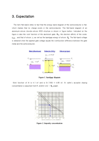 4
4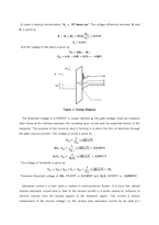 5
5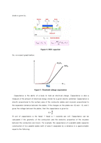 6
6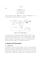 7
7 8
8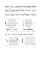 9
9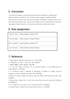 10
10 11
11
추천 연관자료
- 목차
-
목 차
1. Purpose
2. Experiment Procedure
2.1. RCA cleaning
2.1.1 SC-1
2.1.2 SC-2
2.2 Atomic layer deposition (ALD) for Al2O3
2.3 E-beam evaporation for SiO2 and Al gate
2.4 Measurement of C-V and I-V
3. Expectation
4. Results and Discussion
4.1 I-V Measurement
4.2 C-V Measurement
5. Conclusion
6. Role Assignment
7. Reference
- 본문내용
-
The threshold voltage of a MOSFET is usually defined as the gate voltage where an inversion layer forms at the interface between the insulating layer (oxide) and the substrate (body) of the transistor. The purpose of the inversion layer's forming is to allow the flow of electrons through the gate-source junction. The voltage of oxide is given by
V_OX= 1/C_OX 2√(qN_A ε_Si V_0 )
SiO_2 V_OX= 1/C_(SiO_2 ) 2√(qN_A ε_Si V_0 )= 0.52429 V
Al_2 O_3 V_OX= 1/(Al_2 O_3 ) 2√(qN_A ε_Si V_0 ) = 0.20971 V
The voltage of threshold is given by
V_TH= V_FB+V_OX+V_Si= V_FB+ 1/C_OX 2√(qN_A ε_Si V_0 )+ 2V_0
Therefore threshold voltage of SiO_2 MOSFET is 0.22429 V and Al_2 O_3 MOSFET is -0.09029 V.
Saturation current is a term used in relation to semiconductor diodes. It is more fully named reverse saturation current and is "part of the reverse current in a diode caused by diffusion of minority carriers from the neutral regions to the depletion region. This current is almost independent of the reverse voltage." I_s, the reverse bias saturation current for an ideal p-n diode is given by,
Figure 4. MOS capacitor
So, we expect graph bellow.
Figure 5. Threshold voltage expectation
Capacitance is the ability of a body to hold an electrical charge. Capacitance is also a measure of the amount of electrical energy stored for a given electric potential. Capacitance is directly proportional to the surface area of the conductor plates and inversely proportional to the separation distance between the plates. If the charges on the plates are +Q and −Q, and V gives the voltage between the plates, then the capacitance is given by
C= Q/V
SI unit of capacitance is the farad; 1 farad is 1 coulomb per volt. Capacitance can be calculated if the geometry of the conductors and the dielectric properties of the insulator between the conductors are known. For example, the capacitance of a parallel-plate capacitor constructed of two parallel plates both of area A separated by a distance d is approximately equal to the following:
- 참고문헌
-
7. Reference
1. Masao Taguchi, IEEE Electron Device Lett., 12, 642(1992)
2. J. Robertson, Eur. Phys. J. Appl. Phys., 28, 265(2004)
3. 김완돈, 황철성, 차세대 capacitor 기술 개발
4. S.J. Kim, G.H. Chang, Y.S. Byuon, Y.C. Jin, and G.G. Jheong, J. of the Korean Society for Heat Treatment, 6, 204(1993)
5. P. Chowdhurya, Harish C. Barshilia, N. Selvakumar, B. Deepthi, K.S. Rajam, Ayan Roy Chaudhuri, and S.B. Krupanidhi, Physica B, 403, 3718(2008)
6. Gang He, Qi Fang, Liqiang Zhu, Mao Liu, and Lide Zhang, Chemical Physics Letters, 395, 259(2004)
7. Baoxing Zhao, Jicheng Zhou, Yu Chen, and Yinqiao Peng, Journal of Alloys and Compounds 509 4060(2011)
8. C.K. Chung, M.W. Liao, and C.W. Lai, Thin Solid Films 518, 1415(2009)
9. Myung-Hwan An, Journal of the Korean Physical Society, 47, 847(2005)
자료평가
-
아직 평가한 내용이 없습니다.


