


[전자재료실험설계] MOS Capacitor 계획서
 등록일 / 수정일
- 페이지 / 형식
- 자료평가
- 구매가격
- 2011.08.18 / 2019.12.24
- 11페이지 /
 hwp (아래아한글2002)
 - 평가한 분이 없습니다. (구매금액의 3%지급)
- 1,400원
최대 20페이지까지 미리보기 서비스를 제공합니다.
자료평가하면 구매금액의 3%지급!
 1
1 2
2 3
3 4
4 5
5 6
6 7
7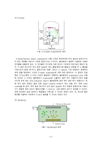 8
8 9
9 10
10 11
11
추천 연관자료
- 목차
-
CONTENTS
1. Subject
2. Object
3. Theory
[1] MOS Capacitor
[2] Leakage current and Capacitance
[3] Thin Film Deposition
1) Chemical Deposition
(1) CVD(Chemical Vapor Deposition)
(2) PECVD(Plasma Enhanced CVD)
2) Physical Deposition
(1) Ion Plating
(2) Thermal Evaporation
(3) Laser Ablation
(4) MBE(Molecular Beam Epitaxy)
(5) E-beam
(6) Sputtering
[4] Photolithography
4. Experiment Process
[1] SiO2, Si3N4 Deposition
[2] Metal Deposition with Photolithography
[3] I-V & C-V Measurement
5. References
- 본문내용
-
[3] Thin Film Deposition
초집적 반도체를 구성하는 소자들은 그 특성상 그 크기가 매우 얇아(작고) 미세한 조직을 가진다. 그리고 이것은 박막 증착(TFD = Thin Film Deposition) 공정을 통해 제작된다. 박막 증착이란 이름 그대로 표면에 얇은 막을 씌우는 기술을 뜻하는데 이 공정을 통해 기판(substrate)이나 이전에 증착된 층에 재료의 얇은 막을 씌워 올린다. MOS의 경우에는 silicon(반도체) 위에 oxide(산화물, 유전체) 그리고 그 위에 metal을 올리는 것이다. 이러한 공정의 종류와 방법은 주로 화학적이냐 물리적이냐에 따라 크게 두 카테고리로 나뉜다.
그림. 4 박막 공정의 종류
1) Chemical Deposition
유체(액체, 기체) precursor(씌우고자 하는 층이 될 잠재 물질)는 고체 표면에서 화학적 변화를 일으켜, 고체 층을 만든다. 유체가 고체 표면을 둘러싸기 때문에 방향에 관계없이 증착은 모든 표면에서 일어난다. 따라서 chemical deposition 기술에 의한 박막은 표면 전체에 걸쳐 두께가 동일하다.
- 참고문헌
-
5. References
· Arthur Beiser. Concepts of Modern Physics. 6th. pp. 160~184
· William D.Callister, Jr& David G.Rethwisch. Fundamentals of Materials Science and Engineering pp. 37~82, 498~507
· Halliday, Resnick, Walker. Fundamentals of Physics. pp. 656~672
· Charles Kittel. Introduction to Solid State Physics. 8th. pp. 185~213
· http://en.wikipedia.org/wiki/Thin_film
· http://en.wikipedia.org/wiki/Chemical_vapor_deposition
· http://en.wikipedia.org/wiki/Plasma_Enhanced_Chemical_Vapor_Deposition
· http://www.cheric.org/proceeding_disk/kiche2002f/GP057.PDF
· http://en.wikipedia.org/wiki/Molecular_beam_epitaxy
· http://en.wikipedia.org/wiki/Sputtering
· http://en.wikipedia.org/wiki/Sputter_deposition
· http://www.tungsten.com/tipsbeam.pdf
· http://www.semipark.co.kr/semidoc/waferfab/thin_film.asp?tm=8&tms=8
· http://en.wikipedia.org/wiki/Photolithography
자료평가
-
아직 평가한 내용이 없습니다.


