- [재무회계] 반도체 산업분석(영문)
semiconductors. The world would be different without semiconductors and would surely be slower. And semi- conductors have also laid the foundation for worldwide networking through the Internet. The development process continues to move ahead. 2. Main productsBroadly speaking, the semiconductor industry is made up of four main product categories:1.Memory: Memory chips serve as temporary storehouses of data and pass information to and from computer devices brains. 2.Microprocessors: These are central processing units that contain the basic logic to perform tasks. 3.Commodity Integrated Ci
- [반도체] PE CVD(Plasma-Enhanced Chemical Vapor Deposition)
PE CVD (Plasma-Enhanced Chemical Vapor Deposition) ContentsIntroductionWhat is the PECVDPlasma etching, Plasma DepositionPlasma process for semiconductorPlasma CVDPE CVD mechanismPE CVD의 7 stepPE CVD 변수 및 특성PE CVD SiN, SiO2 박막PE CVD W, WSI2 박막ReferenceIntroductionPECVD : 전기적 방전을 통해 기체 내에 화학 반응을 일으켜 화학 기상 증착물을 형성시키는 기술 즉, 대기 중에서의 아크 방전과 같은 열 플라즈마 및 저압 글로우 방전과 같은 불평형 플라즈마 혹은 찬 플라즈마이다. 마이크로 일
- [반도체] Plasma Etching Technology
Plasma Etching Technology마이크로소자 연구실반도체공정및재료1. Dry Etch-Plasma-Etching equipment -Dry Etching process2. Dry Etch application to semiconductor 3.SummaryOutline마이크로소자 연구실반도체공정및재료미세 패턴 제작에 있어서 Wet etching 공정이 가지는 한계anisotropy가 낮음, 공정 조절이 어려움, 입자오염Wet Cleaning에 사용Dry Patterning에 사용Dry etch 공정의 도입마이크로소자 연구실반도체공정및재료Dry etch 장비마이크로소자 연구실반도체공정및재료1.
- [반도체] RIE(Reactive Ion Etching)
processing technologies.Inorganic Material LabYonsei Univ.Introduction정확하게 ion-assisted etching 임. Etching 하고자 하는 substrate 를 power electrode 에 놓음Si 과 Cl 또는 Cl2 와는 화학반응으로 SiCl4 형성 -> 아주 늦음여기에 ion bombard 를 시키면 식각속도 증가Inorganic Material LabYonsei Univ.RIE Apparatus(Up) Schematic diagram of apparatus used for RIE in semiconductor processing.(Right) RIE system from Eidgenossische Technishe Hochschule Suiss Federal Institute of Technology(http://www.ifm.ethz.ch/mems/eqrie.htmInorganic Material L
- 물류창고 & 물류네트워크의 이해
Semiconductor (미국 반도체 및 부품생산업체)전 세계 6개 지역의 보관창고를 폐쇄하고 싱가포르에 새로 건설한 중앙 물류센터에서 항공편을 이용해 마이크로칩을 고객에게 운송함으로써, 내쇼널 반도체사(National Semiconductor)는 단 2년 만에 물류비용을 2.5% 절감하고, 운송시간을 47% 감소시켰으며, 매출액을 34%나 증가시켰다.운송수단을 항공기로 전환하면서 내쇼널 반도체의 운송비용은 상당히 증가하였다. 이러한 운송비용의 증가분은 분산된 물류센터를


 등록일 / 수정일
 pptx (파워포인트 2007이상)
 1
1 2
2 3
3 4
4 5
5 6
6 7
7 8
8 9
9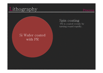 10
10 11
11 12
12 13
13 14
14 15
15 16
16 17
17 18
18 19
19 20
20


