- [신소재공정] Single Crystal 단결성
of the growth processes is possible, which in turn is a key to process improvement.In this experiment, we have to understanding the transport phenomena during crystal growth process by 3 that Growth of single crystal bulk, Growth of single crystal thin film, Growth of single crystal nanowire.2. Theory2.1 Single crystalA single crystal , also called monocrystal, is a crystalline solid in which the crystal lattice of the entire sample is continuous and unbroken to the edges of the sample, with no grain boundaries.Grain boundaries have a lot of significant effects on the mechanical, p
- [박막공학개론] Vacuum Science and Technology(진공과학과 기술)(영문)
the reliability of vacuum, evaluating technique is also important part. In this part, we only concentrate to the generation.Vacuum Characteristics.The First one is clean room. There is no need to make vacuum state if we can keep a clean room. Second is insulating effect. The vacuum can prevents transference of heat. Third is long flight. There are no particles in the vacuum container compare with atmosphere, the air so a particle can fly long distance.Pressure.The unit of vacuum is expressed by the pressure and the pressured is defined as an effect which occurs when a force is applied on
- moype(화합 반도체)
the formation of the single crystal compounds depends on the thermal decomposition of the resctants. details of MOVPE relies on the hydrodynamics and pyrolysis and chemical reaction of reactants inside an reaction chamger. It has been demonstrated that MOVPE is capable of growing virtually all of the Ⅲ-Ⅴ, Ⅱ-Ⅵ, and Ⅳ-Ⅵ compound semiconducters, fabricatinf ultrathin epilayers, forming abrupt heterointerfaces with monolayer transition width, and is suitable for multi-wafer operation yielding a high throughtput. Overview of reactor components and layout, characteristics, and status of
- [신소재설계] Encapsulation을 통한 Oxide TFT의 신뢰성 개선
ThinFilm투과메커니즘Thin Film산소 투과를 막기 위해Passivation 층극성 ↑치밀한 비정질 구조Pin hole의 크기를줄임4해결방안위 메커니즘들을 고려산소/수분 투과에 의한 문제 해결을 위해박막 봉지 물질을 선정 , 특성 분석Thin Film① SiNx② IGZO:N / IGZO③ Vitex 기술MaterialDeposition MethodsubstrateThicknessWVTRUncoated/coateduncoatedCoateda-C:HPECVDPET1501.6140.562.9ta-CFCVAPET1301.6141.41.15AlOxNySputterPET553.890.139SiNxPECVDPEN5502855.6AlOxEbeamPET104.20.1723S
- [공학] 논문분석-The effect of processing parameters on the properties of Ga-doped ZnO thin films by RF magnetron sputtering
화학 흡착에 따른전자 트랩의 발생RESULTS & DISCUSSION고정 조건-구동 압력 : 6mTorr-온도변화: 350℃변수 조건- RF출력100~200WRESULTS & DISCUSSION고정 조건-온도조건 : 350℃-RF 출력 : 175W변수 조건- 구동압력 3.5~7.5mTorr스퍼터링 입자들의 평균 자유 이동경로 감소CONCLUSION다결정 3wt% GZO 박막은 C축 을 우선 면으로 성장모든 GZO박막은 Hexagonal Wurtzite Phase전기적 저항이 제일 낮은 최적의 조건기판 온도- 350℃공정 압력- 6mTorrRF 출력 - 200Wresistivity 3.45*10-4Ωcm


 등록일 / 수정일
 pptx (파워포인트 2007이상)
 1
1 2
2 3
3 4
4 5
5 6
6 7
7 8
8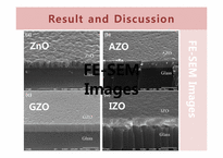 9
9 10
10 11
11 12
12 13
13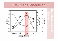 14
14 15
15 16
16 17
17 18
18 19
19


