- [실험] RLC 소자의 이해, CMOS-TTL interface
11(4) 4051(5) Resistor 470Ω, 1㏀, 4.7㏀, 10㏀, 15㏀, 47㏀(6) Power supply, Oscilloscope, Function Generator실험1. CMOS-TTL interface4. 예비 과제(1) TTL 특성과 CMOS 특성을 기술하라.TTL (time-to-live)TTL은 IP 패킷 내에 있는 값으로서, 그 패킷이 네트웍 내에 너무 오래 있어서 버려져야하는지의 여부를 라우터에게 알려준다. 패킷들은, 여러 가지 이유로 적당한 시간 내에 지정한 장소에 배달되지 못하는 수가 있다. 예를 들어, 부정확한 라우팅 테이블의 결합은 패킷을
- [반도체 공정] High-k 물질
inverted state VG : voltage applied to the transistor gate VD : voltage applied to the transistor drain VT : threshold voltageJustification for sustaining/increasing capacitance(2)It can be seen that in this approximation the drain current is proportional to the average charge across the channel with a potential and the average electric field along the channel direction. Initially, ID increases linearly with VD and then eventually saturates to a maximum when VD,sat = VG − VT to yieldThe term (VG − VT) is limited in range due to reliability and room temperature operation constraints,
- VLSI_digital_circuit_design_Add_Shift_Multiplier_layout_simulation
115 vdd gnd 114 62 115 nandX119 vdd gnd 53 117 63 118 119 a2n3X122 vdd gnd a3 120 121 122 a2n2X55 vdd gnd 80 79 54 55 muxX57 vdd gnd 92 91 56 57 muxX73 vdd gnd 72 63 73 norX110 vdd gnd 105 61 109 110 o2n2X113 vdd gnd 84 111 112 113 o2n2X116 vdd gnd 114 62 115 116 o2n2X60 vdd gnd 119 122 60 xorx8 vdd gnd 73 b3 5 andx0 vdd gnd 74 clk p0 dffx1 vdd gnd 113 clk p1 dffx2 vdd gnd 55 clk p2 dffx3 vdd gnd 57 clk p3 dffx4 vdd gnd 116 clk p4 dffx5 vdd gnd 110 clk p5 dffx6 vdd gnd 60 clk p6 dffx7 vdd gnd 5 clk p7 dff.op.tran 0.2n 400n.probe.end26② ** invert
- [국제경영] 핀란드 시장조사-경제, 사회, 문화(영문)
Style and Cultural Features in High/Low Context Communication Cultures:A Case Study of Finland, Japan and IndiaContemporary Finnish Aesthetics(Arto Haapala, University of Helsinki, 2011)http://en.wikipedia.org/wiki/RegionsofFinlandhttp://www.unicef.org/infobycountry/finlandstatistics.htmlhttp://www.kwintessential.co.uk/resources/global-etiquette/finland-country-profile.htmlhttp://www.1uptravel.com/international/europe/finland/topography.htmlhttp://www.geert-hofstede.com http://www.communicaid.com/access/pdf/library/culture/doing-business-in/Doing%20Business%20in%20Finland.pdf


 등록일 / 수정일
 hwp (아래아한글2002)
 1
1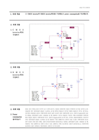 2
2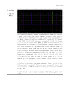 3
3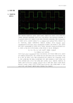 4
4


