- [화학공학]Study of structural and optical properties of Ge and Sn doped ZnO films(영문)
ZnO와 결합한 것 을 알 수있다 그리고 Sn도핑 ZnO는 어닐링에 대한 효과가 나타났다. 1. Introduction ZnO is an important wide-band-gap semiconductor that has a direct band-gap (3.37 eV) with a high exciton binding energy (60 meV), which is greater than the thermal energy at room temperature. Impurity-doping in semiconductors with selective elements greatly affects the basic physical properties, such as the electrical, optical, and magnetic properties, which are crucial for their practical application. Many groups have reported the synthesis of doped ZnO nanoparti
- [화학공학]Carbon-assisted synthesis of aligned Zno nanowires(영문)
of oxygen vacanceis ResultsAnalysis resultsInfluence of exhaustion of Zn gas 600~700℃ 300~400℃ The diameter gradually decreases from the bottom to the top in high temperature zoneResultsAnalysis resultsInfluence of the rate of oxidation 600~700℃ 300~400℃ At high temperature, the diameter of Zno nanowiresis bigger than that at low temperatureConclusionsAligned ZnO nanowires are grown vertically on silicon substrates by carbothermal route Aligned ZnO nanowires are grown without any catalysts and vacuum systemZnO nanowires are grown c-axis direction PL spectrum revea
- [화학공학]Study of structural and optical properties of Ge and Sn doped ZnO films(영문)
Study of structural and optical properties of Ge doped ZnO filmscontentsIntroductionExperimentsResult and discussionConclusionsIntroductionGe is an indirect band gap semiconductor with smaller energy difference between indirect gap and direct gap, and smaller effective masses for electron and hole pairs.Small ionic radius difference between Ge ion and Zn ion.These characteristics lead to the expectation that it is much easier to change the electronic structure around the band edge.ExperimentsA sintered ceramic ZnO target, the surface of which was covered with 3 small area Ge slices
- 양자점(Quantum Dot) Solar Cell
nanowire DSSCs was almost 5 times higherthan DSSCs constructed by upstanding ZnO nanowires.1) Case of DSSCHighly Efficient and Durable Quantum Dot Sensitized ZnO Nanowire Solar Cell Using Noble-Metal-Free Counter ElectrodePhotoelectrode : CdSe/CdS cosensitized ZnO nanowireCounter electrode : ordered mesocellular carbon foam (MSU-F-C)power conversion efficiency : 3.60%,ZnO nanowire Solar CellEffect of ZnO nanowireEffect of ZnO nanowireZnO Nanostructures for Dye-Sensitized Solar Cells, Qifeng Zhang, Christopher S. Dandeneau, Xiaoyuan Zhou, and Guozhong Cao, Advanced MaterialsSynthesi
- [화학공학]계층 구조를 가지고 있는 ZnO 나노구조의 합성과 특징(영문)
and composed of hexagonal-shaped nanowires with a great number of Zn and little oxidation.∙ SEM and HRTEM reveal that individual hierarchical ZnO nanostructures consist of central axial ZnO nanowire and radially oriented ZnO nanorods with 6-fold structural symmetries.∙ The corresponding SAED analyses show that single crystal ZnO nanorods epitaxially grow from the side-wall of central axial ZnO nanowires.∙ The present achievements of hierarchical pure ZnO nanostructures may have potential applications in multichannel optoelectronic devices due to the large surface area and high integr


 등록일 / 수정일
 pptx (파워포인트 2007이상)
 1
1 2
2 3
3 4
4 5
5 6
6 7
7 8
8 9
9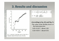 10
10 11
11 12
12 13
13 14
14


