


OTFT(Organic Thin Film Transistor) 실험결과
 등록일 / 수정일
- 페이지 / 형식
- 자료평가
- 구매가격
- 2010.08.14 / 2019.12.24
- 22페이지 /
 ppt (파워포인트 2003)
 - 평가한 분이 없습니다. (구매금액의 3%지급)
- 1,800원
최대 20페이지까지 미리보기 서비스를 제공합니다.
자료평가하면 구매금액의 3%지급!
 1
1 2
2 3
3 4
4 5
5 6
6 7
7 8
8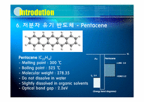 9
9 10
10 11
11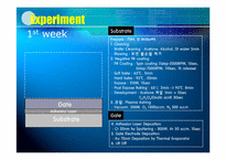 12
12 13
13 14
14 15
15 16
16 17
17 18
18 19
19 20
20- 목차
-
1,Introduction
2, Experiment
3, Analysis
4,Reference
- 본문내용
-
실험목적
Organic Material을 이용하여 Semiconductor Layer와 Dielectric Layer를 증착시켜 봄으로써 Organic TFT 제작 공정을 이해한다.
VT, Mobility, On-off ratio를 통해 제품 특성을 평가하고 유기물과 무기물로 증착한 Dielectric Layer의 차이를 비교해 볼 수 있다.
Pentacene (C22H14)
- Melting point : 300 ℃
- Boiling point : 525 ℃
- Molecular weight : 278.35
- Do not dissolve in water
- Slightly dissolved in organic solvents
- Optical band gap : 2.2eV
Prepare : PI#4, Si Wafer#4
1. Cleaning
∙ Wafer Cleaning : Acetone, Alcohol, DI water 5min
∙ Blowing : 표면 불순물 제거
2. Negative PR coating
∙ PR Coating : Spin coating (1step-2000RPM, 10sec,
2step-7000RPM, 110sec, 1h release)
∙ Soft bake : 65℃, 5min
∙ Hard bake : 95℃, 20min
∙ Expose : 310W, 15sec
∙ Post Expose Baking : 65℃ 2min -> 95℃ 8min
∙ Development : Acetone 계열 1min + 10sec C2H2O4(Oxalic acid) 30sec
3. 관찰, Plasma Ashing
: Vacuum, 500W, O2 1500sccm, N2 500 sccm
4. Adhesion Layer Deposition
∙ Cr 20nm by Sputtering - 800W, Ar 50 sccm, 10sec
5. Gate Electrode Deposition
∙ Au 70nm Deposition by Thermal Evaporator
6. Lift Off
- 참고문헌
-
유기전자소자 OTFT, 전자통신동향분석, 제 20권 5호, 2005년 10월
유기전자공학의 연구현황과 시장전망, 송정근 교수, 동아대학교 전자공학과
OTFT를 이용한 All Organic Display의 연구동향, 도이미, 최종선
Stretchable and foldable silicon integrated circuit, 안종현
TFT-LCD 제조공정 및 기술
Sol-Gel법을 이용한 박막제조, 이진홍, 경북대학교 무기재료 공학과
Organic Thin Film Transistors, Materials, Processed and Devices, B.Chandar Shekar, Jiyeon Lee and Shi-Woo Rhee
자료평가
-
아직 평가한 내용이 없습니다.
오늘 본 자료
더보기
최근 판매 자료
- [화학실험] 아스피린 합성
- 일본의 음식문화 일본 음식 한국 일본 음식 공통점 한국 일본 음식 차이점
- [[AVR 푸쉬업 카운터 만들기]]초음파 센서,거리측정,HC-SR04,AVR,ATmega,회로도,소스코드,졸업작품
- [건축공학] 철골구조 및 철골구조물 사례 조사
- [금오공대 A+] 일물실 음파의 맥놀이 예비보고서 + 결과보고서
- 화학공학과 전공면접, 전공 PT 질문 모음(건설, 엔지니어링, 석유화학, 정유)
- Polymer Substrate for Flexible TFT
- [심리학] 꿈의이론과해석A+
- 회로이론1 이정훈 년도 표기 X
- [혜성] 혜성이 가지는 의의, 혜성의 본체, 혜성의 종류, 혜성의 기원과 종말에 관한 분석

저작권 관련 사항 정보 및 게시물 내용의 진실성에 대하여 레포트샵은 보증하지 아니하며, 해당 정보 및 게시물의 저작권과 기타 법적 책임은 자료 등록자에게 있습니다. 위 정보 및 게시물 내용의 불법적 이용, 무단 전재·배포는 금지됩니다. 저작권침해, 명예훼손 등 분쟁요소 발견시 고객센터에 신고해 주시기 바랍니다.


