


[반도체공정] 미래 리소그래피(lithography) 동향(영문)
 등록일 / 수정일
- 페이지 / 형식
- 자료평가
- 구매가격
- 2011.06.08 / 2019.12.24
- 13페이지 /
 docx (MS워드 2007이상)
 - 평가한 분이 없습니다. (구매금액의 3%지급)
- 1,400원
최대 20페이지까지 미리보기 서비스를 제공합니다.
자료평가하면 구매금액의 3%지급!
 1
1 2
2 3
3 4
4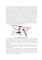 5
5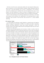 6
6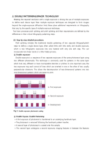 7
7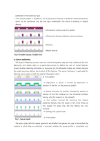 8
8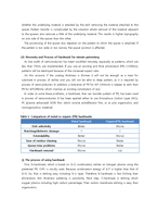 9
9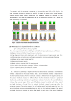 10
10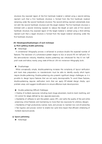 11
11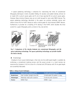 12
12 13
13
추천 연관자료
- 목차
-
The chip makers are still using a 193 nm lithography tool with an immersion technology. However, the next-generation lithography tool is still not available and they have to continue the scaling of the devices. Therefore, this essay aims to know about trend of the future lithography and requirement of that, and also know about the double patterning, Spacer patterning which are currently spotlighted.
Contents
The general future trend of the lithography and technical requirements
Lithography technology
Photo resist (materials, sensitivities)
Optical mask
Double patterning
EUV mask
Imprint template
Conclusion (>16nm, <16nm)
DOUBLE PATTERNING/SPACER TECHNOLOGY
Step-by-step detailed procedures
Double exposure
Double Expose, Double Patterning
Spacer patterning
Necessity and Process of Hardmask for minute patterning
Material/process requirements for the hardmasks
Advantages/disadvantages of each technique
Pitch-splitting double-patterning
Spacer patterning
- 본문내용
-
(4) Double patterning
The double patterning is divided into four parts, leading with wafer requirements and then two sets of lithographic requirements (Generic Pitch Splitting - Double Patterning Requirements Driven by MPU metal Half-Pitch and Generic Spacer Patterning Requirements - Driven by Flash). The lithography requirements are different for each process; the requirements for pitch splitting are based on the MPU metal half-pitch. The fundamental premise is that both the line and the space must meet the 12% CD specification. Since the space depends on the overlay and printed line width, meeting the 12% specification drives the overlay specification for double pattering. Further, to make the overlay specification as large as possible, the line width needs to be controlled to the tightest possible. In the tables, this means the double patterning line width must be controlled to the specification that an MPU gate line width would be controlled to. The mask specifications needed to support this specification are shown in the bottom rows. The matched double patterning mask image placement must be tighter than a single mask overlay by the square root of 2. Therefore, the mask-to-mask overlay contribution in any particular location must be 20% of the total pitch splitting error budget. The wafer CD error budgets for spacer patterning are also driven by the need to have both the line and space w
자료평가
-
아직 평가한 내용이 없습니다.


