


[반도체 공정 설계] 반도체 소자 제조공정(Semiconductor Device Fabrication Process)(영문)
 등록일 / 수정일
- 페이지 / 형식
- 자료평가
- 구매가격
- 2011.06.08 / 2019.12.24
- 12페이지 /
 hwp (아래아한글2002)
 - 평가한 분이 없습니다. (구매금액의 3%지급)
- 1,400원
최대 20페이지까지 미리보기 서비스를 제공합니다.
자료평가하면 구매금액의 3%지급!
 1
1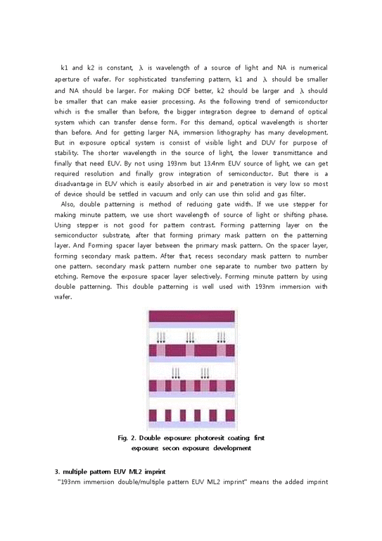 2
2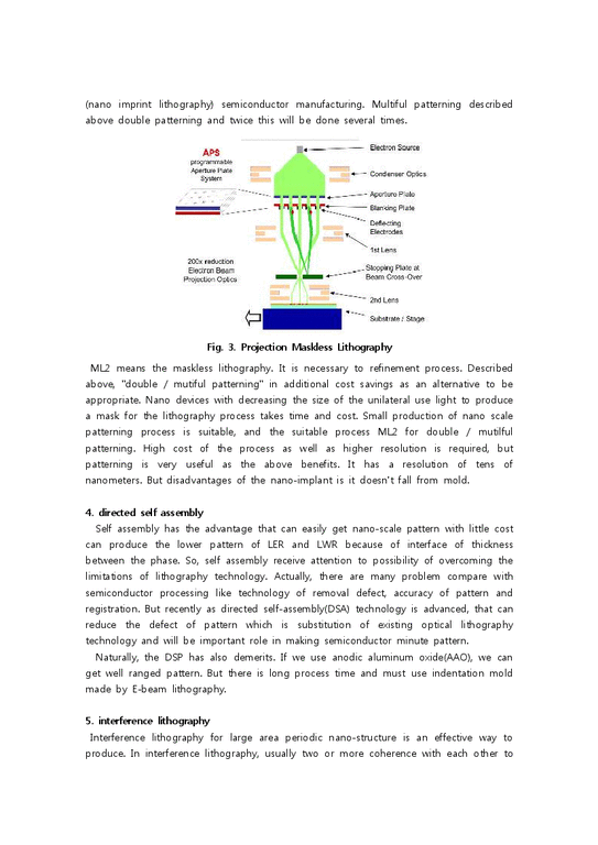 3
3 4
4 5
5 6
6 7
7 8
8 9
9 10
10 11
11 12
12
추천 연관자료
- 목차
-
Ⅰ. the general future trend of the lithography and technical requirements.
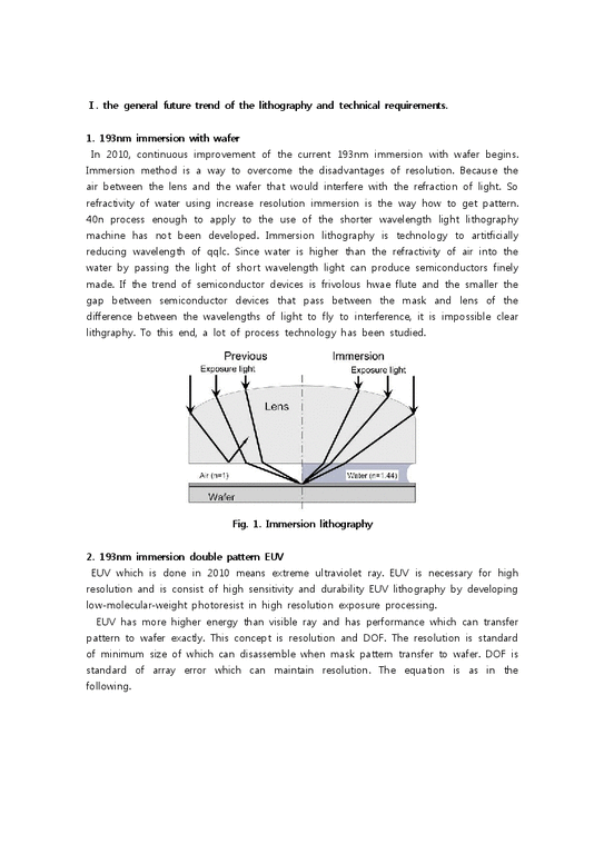
1. 193nm immersion with wafer
2. 193nm immersion double pattern EUV
3. multiple pattern EUV ML2 imprint
4. directed self assembly
5. interference lithography
Ⅱ. "Pitch Splitting (Double Exposure and Double Patterning)" and "Spacer Patterning"
1. Pitch splitting
2. Spacer Patterning Technology
Ⅲ. Reference
- 본문내용
-
ML2 means the maskless lithography. It is necessary to refinement process. Described above, "double / mutiful patterning" in additional cost savings as an alternative to be appropriate. Nano devices with decreasing the size of the unilateral use light to produce a mask for the lithography process takes time and cost. Small production of nano scale patterning process is suitable, and the suitable process ML2 for double / mutilful patterning. High cost of the process as well as higher resolution is required, but patterning is very useful as the above benefits. It has a resolution of tens of nanometers. But disadvantages of the nano-implant is it doesn't fall from mold.
4. directed self assembly
Self assembly has the advantage that can easily get nano-scale pattern with little cost can produce the lower pattern of LER and LWR because of interface of thickness between the phase. So, self assembly receive attention to possibility of overcoming the limitations of lithography technology. Actually, there are many problem compare with semiconductor processing like technology of removal defect, accuracy of pattern and registration. But recently as directed self-assembly(DSA) technology is advanced, that can reduce the defect of pattern which is substitution of existing optical lithography technology and will be important role in making semiconductor minute pattern.
Naturally, the DSP has also demerits. If we use anodic aluminum oxide(AAO), we can
- 참고문헌
-
Ⅲ. Reference
[1] A Spacer Patterning Technology for Nanoscale CMOS. Yang-Kyu Choi, Tsu-Jae King, Member, IEEE, and Chenming Hu, Fellow, IEEE. IEEE TRANSACTIONS ON ELECTRON DEVICES, VOL. 49, NO. 3, MARCH 2002.
[2] Strategies for nanoelectronics. G.F. Cerofolini. Microelectronic Engineering 81 (2005) 405–419.
[3] Spacer defined FinFET: Active area patterning of sub-20 nm fins with high density. B. Degroote, R. Rooyackers. Microelectronic Engineering 84 (2007) 609–618.
[4] Sub 50-nm FinFET: PMOS. Xuejue Huang, Wen-Chin Lee, Charles Kuo. Department of Electrical Engineering and Computer Sciences, University of California at Berkeley, CA 94720 USA (revised 12/9/1999)
[5]Split and Design Guidelines for Double Patterning - Vincent Wiauxa, Staf Verhaegena, Shaunee Chenga, Fumio Iwamotob, Patrick Jaenena, Mireille Maenhoudta, Takashi Matsudab, Sergei Postnikovc, Geert Vandenberghea[6]Layout Decomposition for Double Patterning Lithography - Andrew B. Kahng, Chul-Hong Park, Xu Xu, and Hailong Yao Blaze DFM, Inc., Sunnyvale, CA
http://en.wikipedia.org/wiki/Double_patterning
자료평가
-
아직 평가한 내용이 없습니다.


