


[공학] thin films on pre-deposited ZnO-glass Substrates by RF Sputtering Technique(영문)
 등록일 / 수정일
- 페이지 / 형식
- 자료평가
- 구매가격
- 2010.11.09 / 2019.12.24
- 5페이지 /
 docx (MS워드 2007이상)
 - 평가한 분이 없습니다. (구매금액의 3%지급)
- 800원
최대 20페이지까지 미리보기 서비스를 제공합니다.
자료평가하면 구매금액의 3%지급!
 1
1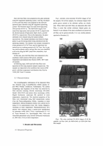 2
2 3
3 4
4 5
5
추천 연관자료
- 목차
-
ABSTRACT
1. Introduction
2. Experimental
2.1. Film preparation
2.2. Characterization
3. Results and Discussion
3.1 Structural Properties
3.2 Surface morphology
3.3 optical properties
3.4 Electrical Properties
4. Conclusions
References
- 본문내용
-
2. Experimental
2.1. Film preparation
Pure ZnO thin films were prepared on the glass substrate using RF magnetron sputtering system. And Mg, Ga doped (3 wt%) ZnO thin films were prepared on the ZnO pre-sputtered glass substrate using RF magnetron sputtering system. The PureZnO target was made from high purity ZnO powder (99.99 %) . The MZO/GZO targets were made from high purity ZnO powder (99.99 %) doped with the desired amount of high purity MgO, Ga2O3, powder (99.99 %), respectively. Prior to the deposition, the glass substrates were cleaned using the typical method, successively. The cleaned substrates were blown by high purity N2 gas for drying before being introduced into the sputtering chamber. The chamber was initially evacuated to a base pressure of 4.9*10-6Torr, and the deposition was carried out at a working pressure of 6*10-3Torr. The Ar gas was used as plasma source and gas flow rate was controlled at 40 sccm using the MFC (mass flow controller). And distance of
In first step, pure ZnO thin films were deposited in the conditions which consist of RF power, substrate temperature and duration time fixed at 200W, 300 °Cand 20 minutes.
In following steps, MZO and GZO thin films were deposited on first-step prepared samples respectively. The samples are deposited in the conditions that consist of RF power, substrate temperature and duration time fixed at 150W,200 °Cand 15 minutes.
2.2. Characterization
The crystallographic information of the deposited films was obtained using X-raydiffraction (XRD) spectra (X’ pert PRO, Phillips. Eindhoven, Netherlands). The surface morphology and roughness of the films was observed by field emission scanning electron microscopy (FE-SEM, Model: JSM-6701F) and atomic force microscopy (AFM, Digital Instrument, nanoscope III) operated at room temperature, respectively. The electrical properties of the films were determined using Hall measurement system (Van der Pauwconfiguration, Hilton, Australia) at room temperature. Optical absorption studies were carried out by using UV-Vis spectrometer (Cary 100, Varian, Mulgrave, Australia) at room temperature. Photoluminescence (PL) spectra were obtained using a closed-cycle liquidhelium cry generator (APD, SH-4, USA), a spectrometer (f = 0.5 m, Acton Research Co., Spectrograph 500i, USA) and intensified photodiode array detector (Princeton Instrument co., IRY1024, USA) at room temperature.
3. Results and Discussion
3.1 Structural Properties
Fig.1. presents cross-sectional FE-SEM images of all the samples. For all the samples, the columnar shaped ZnO grains grown normal to the substrate surface are clearly seen. When MZO and GZO films are deposited after ZnO films, it seems that similar columnar shaped grains are formed. It can indicate if the same conditions are preserved, all films can be grownvertically. It is very similar patterns reported in literature [1].
- 참고문헌
-
[1] C.C. Liu, Y.S. Chen, J.J. Huang, Electron. Lett.42/14 (2006) 824.
[2] B. Asenjo, A.M. Chaparro, M.T. Gutiérrez, J. Herrero, J. Klaer, Thin Solid Films 515/15
(2007) 6036.
[3] I. Hamberg, C.G. Granqvist, J. Appl. Phys. 60/11 (1986).
[4] T. Minami, Semicond. Sci. Technol. 20/4 (2005).
[5] Z.L. Pei, X.B. Zhang, G.P. Zhang, J. Gong, C. Sun, R.F. Huang, L.S. Wen, Thin Solid
Films 497/1-2 (2006) 20.
[6] H.J. Ko, Y.F. Chen, S.K. Hong, H. Wenisch, T. Yao, D.C. Look, Appl. Phys. Lett. 77/23
(2000) 3761.
[7] C.S. Hong, H.H. Park, J. Moon, H.H. Park, Thin Solid Films 515/3 (2006) 957.
[8] S.J. Henley, M.N.R. Ashfold, D. Cherns, Surf. Coat.Technol. 177-178 (2004) 271.
[9] J.H. Lee, S.Y. Lee, B.O. Park, Mater. Sci. Eng.: B 127/2-3 (2006) 267.
[10] J.H. Lee, B.O. Park, Thin Solid Films 426/1-2 (2003) 94.
자료평가
-
아직 평가한 내용이 없습니다.


