


[화학공학]Study of structural and optical properties of Ge and Sn doped ZnO films(영문)
 등록일 / 수정일
- 페이지 / 형식
- 자료평가
- 구매가격
- 2010.08.20 / 2019.12.24
- 10페이지 /
 pptx (파워포인트 2007이상)
 - 평가한 분이 없습니다. (구매금액의 3%지급)
- 1,200원
최대 20페이지까지 미리보기 서비스를 제공합니다.
자료평가하면 구매금액의 3%지급!
 1
1 2
2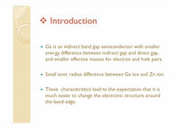 3
3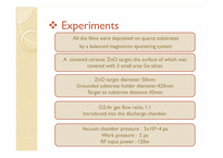 4
4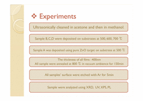 5
5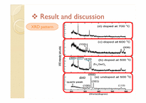 6
6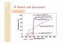 7
7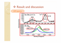 8
8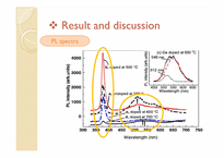 9
9 10
10
추천 연관자료
- 목차
-
1 Introduction
2 Experiments
3 Result and discussion
4 Conclusions
- 본문내용
-
Ge is an indirect band gap semiconductor with smaller energy difference between indirect gap and direct gap, and smaller effective masses for electron and hole pairs.
Small ionic radius difference between Ge ion and Zn ion.
These characteristics lead to the expectation that it is much easier to change the electronic structure around the band edge.
- The effects of doping and substrate temperature on the structural and optical properties of the Ge doped ZnO films were investigated by XRD, XPS, UV, PL
- The XRD patterns show that Zn2GeO4 phase was formed in the films and the crystallization of ZnO deteriorates
- The enhancement of UV light emission at about 380nm may be caused by excitons which were formed at the interface between Zn2GeO4 and ZnO grains.
- The PL spectrum show that some Ge2+ should replace the Zn2+ positions during the Zn2GeO4 grains growth and form the Ge2+ luminescence centers in Zn2GeO4 grains.
자료평가
-
아직 평가한 내용이 없습니다.
오늘 본 자료
더보기
최근 판매 자료
- LED기술 레포트
- LED에 모든것 레포트
- 아보가드로 상수 구하기
- 냉동만두의 HACCP시스템에 있어서의 효과적인 검증방법
- 유전자가위 기술 원리, 특징, 활용 및 향후전망 [유전자가위,유전자,유전자 치료,제한효소,징크핑거,탈렌,크리스퍼]
- 물리 실험 포사체운동 실험 [결과]
- [A+ 45 예비레포트,PSpice포함] 기초전자공학실험 - 차동 증폭기 회로
- [디지탈전자회로,전자공학] 디지탈전자회로 핵심요약정리
- [분석화학실험] report 6 Determination of chloride , the Fajans method
- 비디오 대여 시스템 배경도, 자료흐름도 그리기

저작권 관련 사항 정보 및 게시물 내용의 진실성에 대하여 레포트샵은 보증하지 아니하며, 해당 정보 및 게시물의 저작권과 기타 법적 책임은 자료 등록자에게 있습니다. 위 정보 및 게시물 내용의 불법적 이용, 무단 전재·배포는 금지됩니다. 저작권침해, 명예훼손 등 분쟁요소 발견시 고객센터에 신고해 주시기 바랍니다.


