


[반도체] Molecular Beam Epitaxy(MBE)
 등록일 / 수정일
- 페이지 / 형식
- 자료평가
- 구매가격
- 2010.04.26 / 2019.12.24
- 19페이지 /
 ppt (파워포인트 2003)
 - 평가한 분이 없습니다. (구매금액의 3%지급)
- 1,800원
최대 20페이지까지 미리보기 서비스를 제공합니다.
자료평가하면 구매금액의 3%지급!
 1
1 2
2 3
3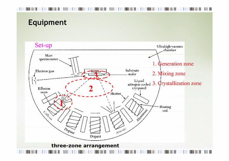 4
4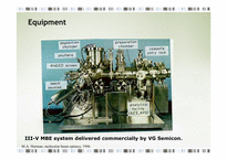 5
5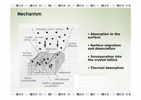 6
6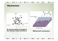 7
7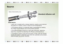 8
8 9
9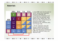 10
10 11
11 12
12 13
13 14
14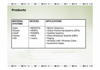 15
15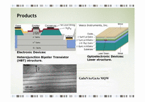 16
16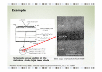 17
17 18
18 19
19
추천 연관자료
- 목차
-
Introduction
Equipment
Processes
sources
materials
parameters
interface
mechanism
Products
Example
Summary
- 본문내용
-
Solid Source
each cell is loaded with a charge material, usually a pure element like gallium or arsenic, which is solid at room temperature.
The gaseous atomic or molecular beam is generated by heating the charge in the effusion cell in the growth chamber.
The effective beam pressure or flow rate of the gas, called the beam flux, is varied by adjusting the effusion cell temperature.
A shutter is used to “shut off” the beam; in fact, with the shutter closed, the beam is deflected away from the substrate and pumped away through the growth chamber.
Gas Source
CBE (Chemical Beam Epitaxy)
MOMBE (Metal-organic MBE)
GS-MBE (Gas Source MBE)
the charge material - a molecular species that contains the desired element - is a gas at room temperature. (Liquids with an appreciable vapor pressure at or near room temperature may also be used.)
A standard gas handling system connects the external gas canister to the growth chamber.
Beam fluxes may be changed almost instantly by adjusting the gas flow valves. When the valve is closed, no charge material enters the chamber.
The source used to introduce the gas may be a "cracker" which is used to thermally decompose the gas, e.g. . Or it may be an "injector" which operates at a sufficiently high temperature to prevent condensation and maintain a stable flux
- 참고문헌
-
M.A. Herman, molecular beam epitaxy, 1996
2. Sze, Semiconductor device, 2002
3. Carl Wilmsen et al, vertical-cavity surface-emitting lasers, 1999
4. Sarah Kurtz et al, applied physics letters, vol. 78, no. 6, 2001
5. M.A. Pinault et al, applied physics letters, vol. 78, no. 11, 2001
6. Masahiko Kondow et al, IEEE J. selected topics in quantum electronics, vol. 3 no. 3 1997. S.M
자료평가
-
아직 평가한 내용이 없습니다.
오늘 본 자료
더보기
최근 판매 자료
- 심슨의 역설은 무엇인지(발생 원인 포함) 기술하고 우리 주위에서 발생한 사례를 찾아 요약 그 역설을 해결하여 올바로 해석
- 조명 디스플레이 - LED에 대해서
- [발광다이오드, LED, OLED, 플라스틱발광다이오드] 발광다이오드(LED)의 정의, 발광다이오드(LED)의 종류와 국내 발광다이오드(LED) 관련 사례 및 유기발광다이오드(OLED), 플라스틱발광다이오드(LED)에 관한 분석
- LED조명의 이해
- [열역학] 냉장고 증발기 시스템 열 효율성 고찰
- 충북대_일반물리학및실험1_7주차_역학적에너지보존
- [A+] razavi 마이크로 전자회로 4장 솔루션
- [실험] 전기용량과 유전율 측정
- 상하수도공학(구미서관) 연습문제 2장
- 이재수 수문학(구미서관) 연습문제 6장

저작권 관련 사항 정보 및 게시물 내용의 진실성에 대하여 레포트샵은 보증하지 아니하며, 해당 정보 및 게시물의 저작권과 기타 법적 책임은 자료 등록자에게 있습니다. 위 정보 및 게시물 내용의 불법적 이용, 무단 전재·배포는 금지됩니다. 저작권침해, 명예훼손 등 분쟁요소 발견시 고객센터에 신고해 주시기 바랍니다.


